12-port S-Video/Audio Switch
Introduction
I have an old CRT with a few old video game consoles and a VCR connected to it by S-Video. I had been using a cheap 4-port passive A/V switch to multiplex them into the TV, but in 2020 I had outgrown the 4 ports it provided.
Cheap S-Video products are notorious for compromising video signals, so I wasn’t keen on daisy chaining switches together. Instead, I decided to build my own active switch that would amplify the video signals and provide more inputs than I would ever need. That took me about 4 months from start to finish and introduced me to several new disciplines along the way.
All of the design files and code are in the Github repository.
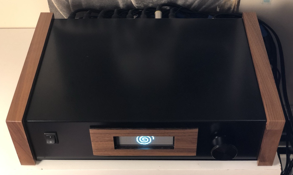
There are photos and a video demo of the completed device in the conclusion, if you want to skip straight to it.
Planning
Interface
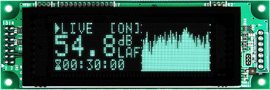
Consumer switches typically have a button for each input, but I thought that would be a little unwieldy with a lot of inputs. Each button would at least need to be labeled to keep track of what was connected to each input, so why not use a microcontroller and a display to keep track of the inputs? I envisioned a VFD (Vacuum Fluorescent Display) with a flashy graphical menu and an iPod-inspired knob for navigating it.
I think The Right Way to do this would be to detect active input signals and auto-switch. I don’t have a good excuse for not going that route except that I’ve always wanted to use a VFD in a project. They are really striking displays.
Electronics
I’m really a beginner when it comes to analog electronics, but fortunately there are monolithic parts that do the hard parts I needed for this project.
For switching the audio signals, I selected the ADG1606 16-channel analog multiplexer. For the video signals, I prototyped a design using ADG1206 16-channel analog multiplexers, but I ended up using the MAX4315 8-channel video multiplexer-amplifier instead because it required fewer external passives.
I’ve always been intimidated by power supplies, and both of the analog multiplexer ICs are dual-supply and need negative voltage reference inputs. I obtained the +5V and -5V I needed by feeding +/-5V regulators with the outputs from a +/-12V DC-to-DC converter powered by a 12V wall wart. More on that later…
For the interface, I ordered a 140x32 VFD from Noritake with full-display dimming, and I planned to use a rotary encoder to detect knob rotation.
Everything is controlled by an ATMEGA2561.
Enclosure
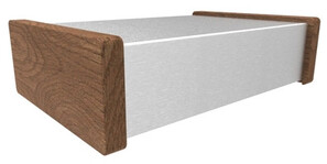
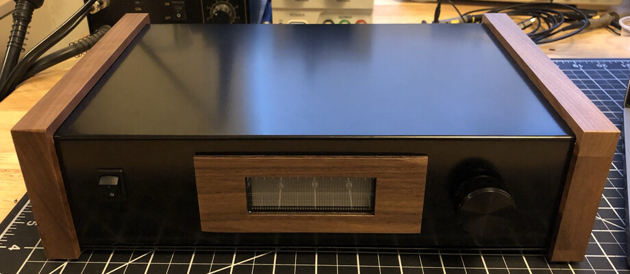
I would need an enclosure large enough to accommodate all of the input and output connectors, and I would need to be able to modify the front panel to install a power switch, the display, and the knob. I set out to find a plastic enclosure, but when I saw this 12 in x 8 in x 3 in aluminum case with walnut panels from Hammond manufacturing, I knew it was the one. I am a sucker for wood paneling.
The last (and only other) time I modded an enclosure it was a bit of a hack job, and I was a little skeptical of my ability to work with a metal one.
Number of inputs
After making some decisions on the electronic components and enclosure, I decided to build the switch to support 12 inputs. 12 is large enough that I can’t imagine having that many S-Video devices, but small enough that the necessary S-Video and RCA connectors would fit into a reasonable physical space.
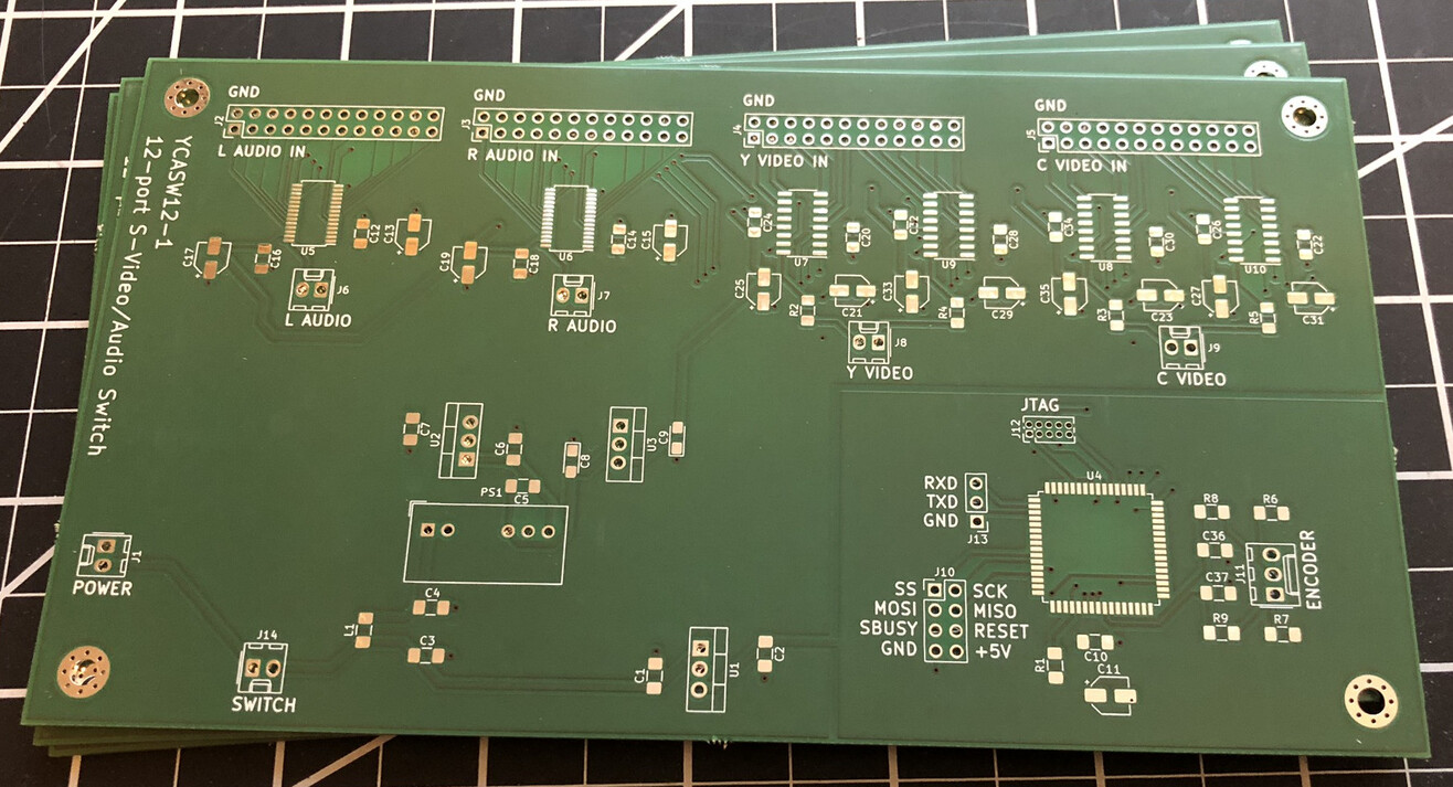
PCB design
This is only the second board I’ve designed, and I am still getting the hang of it. As a software developer I find it a little unnerving to commit time and money to have boards manufactured before being able to fully test the design. I expected to make some bodges.
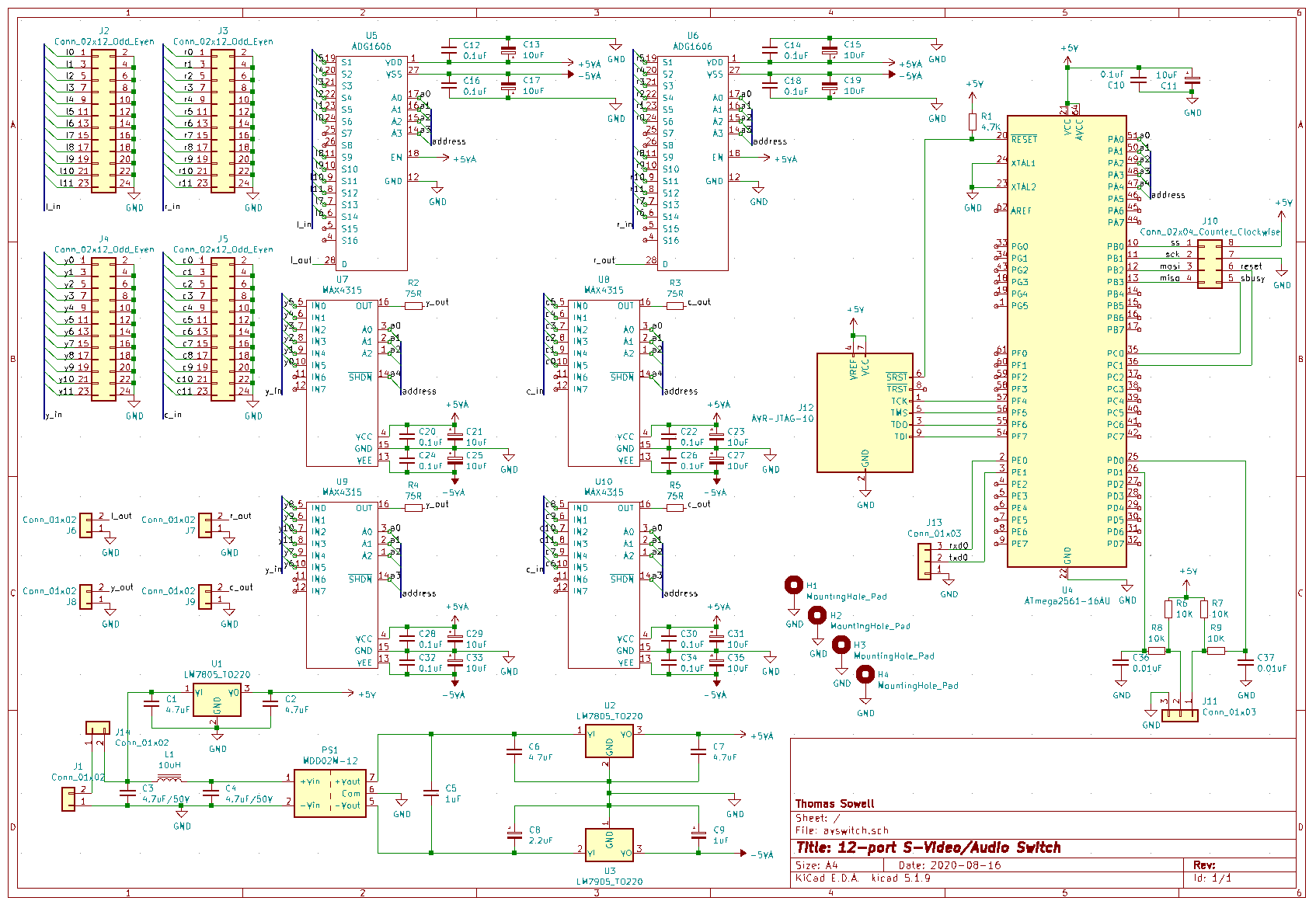
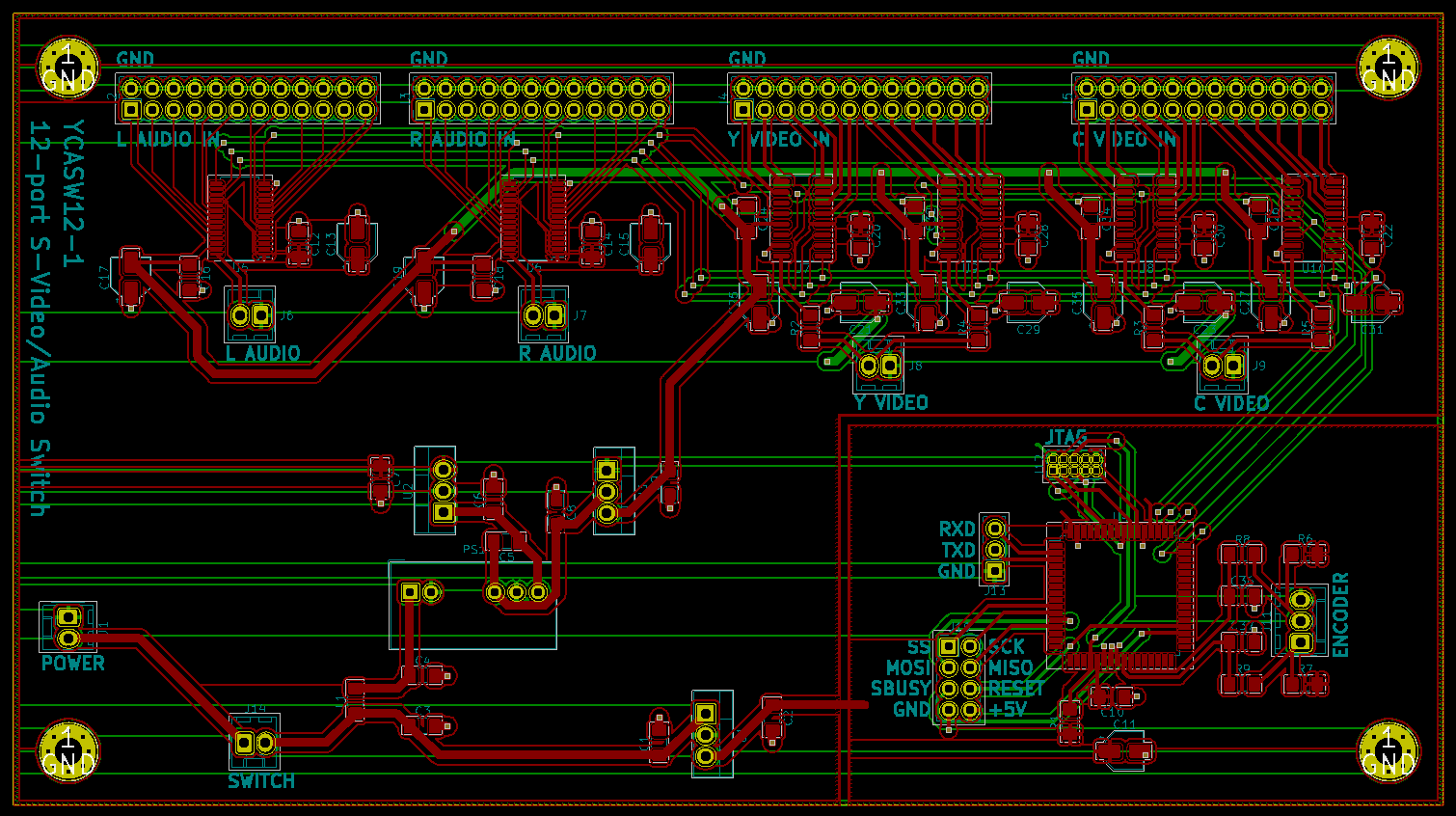
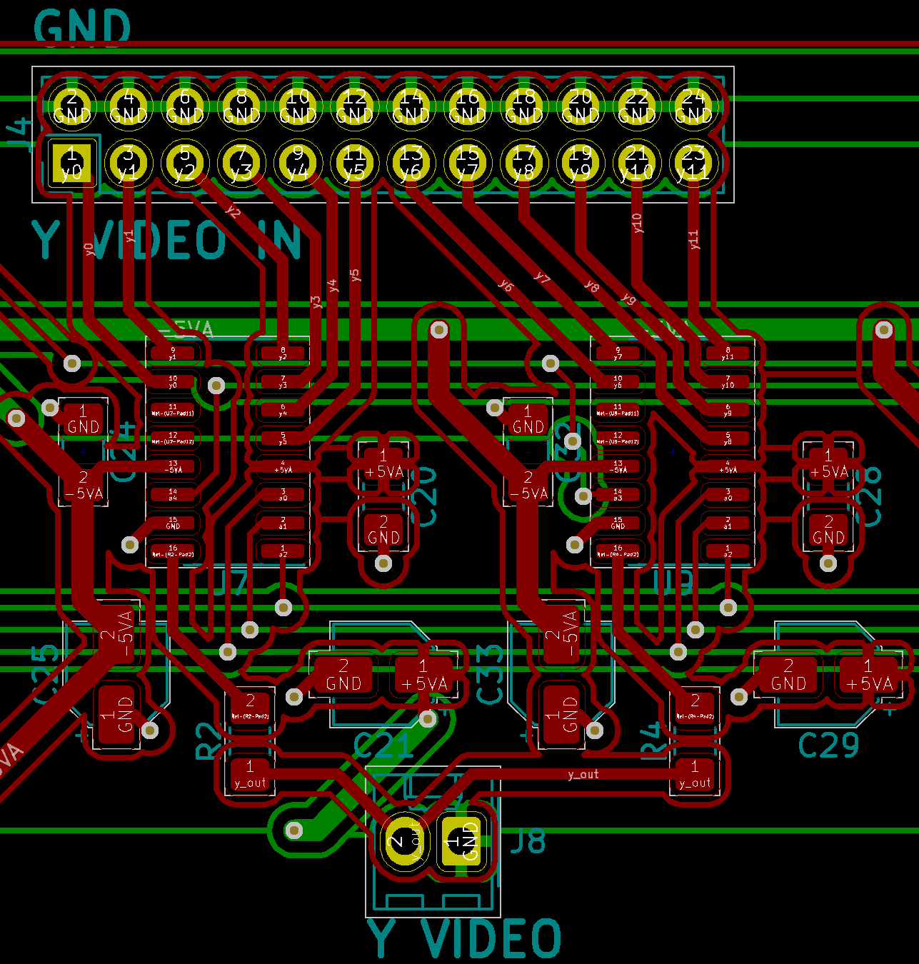
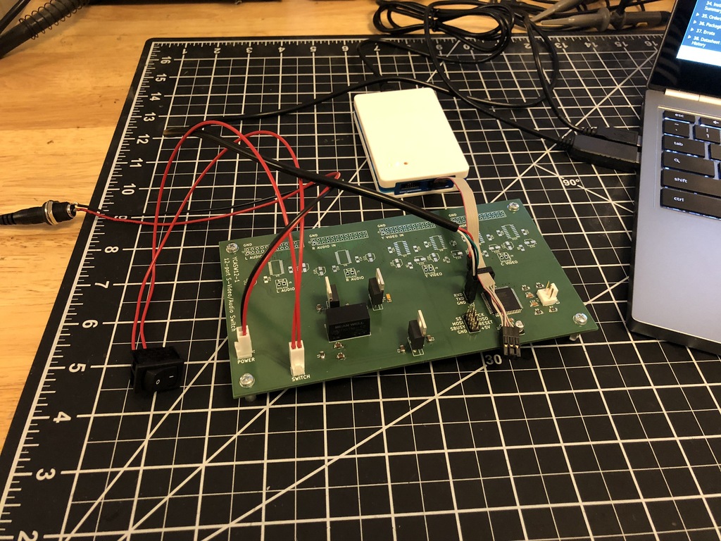
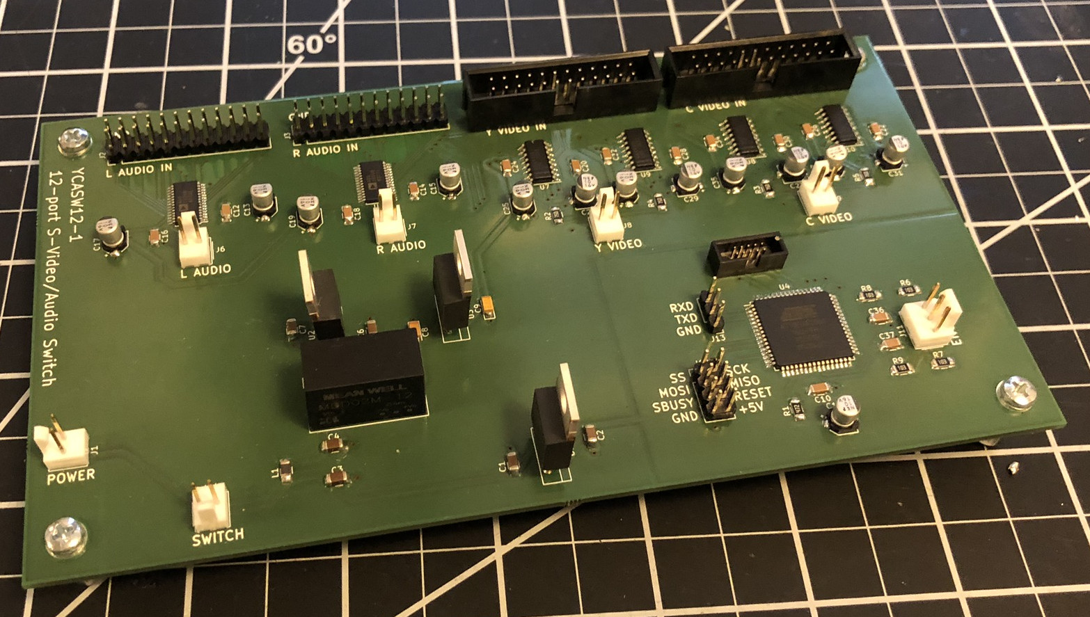
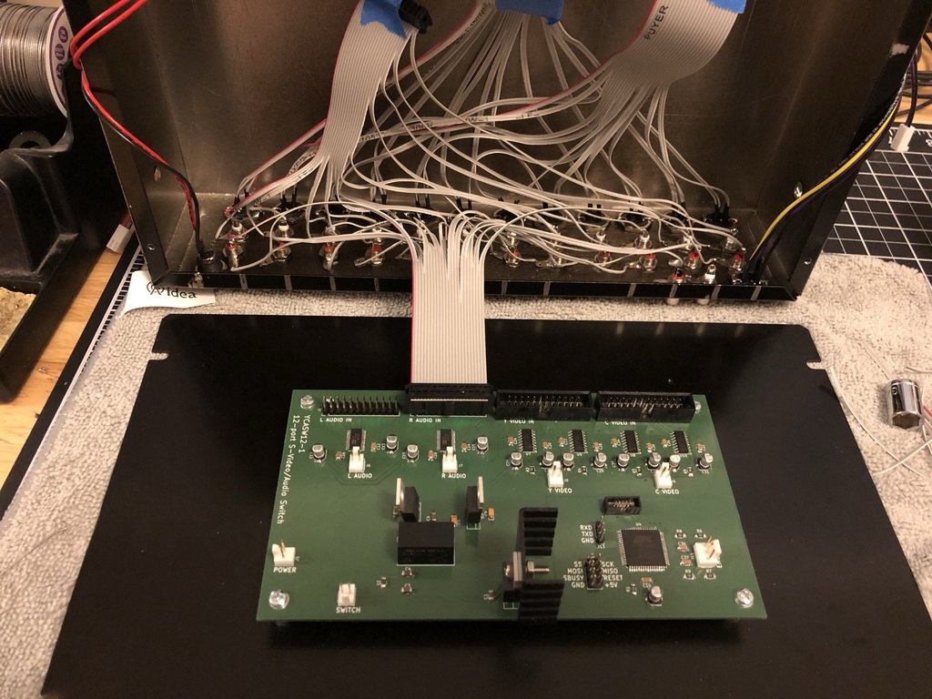
The board is roughly divided into quadrants. The lower left has power supply components, the lower right is the digital area with the microcontroller, SPI header to connect to the VFD display, and rotary encoder connector and debouncing circuit. The upper right multiplexes the video luminance and chroma video inputs, and the upper left multiplexes the left and right audio inputs.
There is a 24-pin header for each of the left audio, right audio, luminance, and chroma inputs. Ribbon cables soldered to the panel connectors connect to these input headers. Each of the four corresponding outputs has a two-pin connector running in a rough horizontal line across the middle of the board.
I tried to baby the video traces to ensure signal integrity. I used larger traces for the signals and avoided routing any video signals through vias. Interleaving the ground wires in the ribbon cables should help too. I also separated the analog parts of the circuit from the digital parts and gave them separate +5V regulators and ground planes.
Addressing
In order to avoid vias for the video signals, I based the order in which the inputs are connected to the multiplexers on the location of the input pins on the package instead of their symbolic input number.
The MAX4315 only multiplexes 8 inputs, so I had to use two banks of them to support 12 inputs. Rather than use hardware decoding using a NOT gate on the /SHDN pins of one bank, I just connected a different address pin to each bank, so the microcontroller has to keep a4 the inverse of a3.
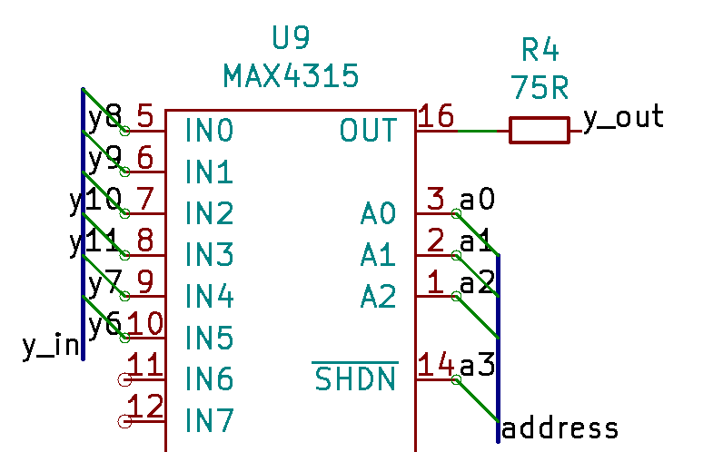
The inputs in order from 1 to 12 are addressed in this not-at-all-confusing order:
0x15 0x14 0x13 0x12 0x11 0x10 0x0D 0x0C 0x08 0x09 0x0A 0x0B
At least that can be fixed in software.
Construction
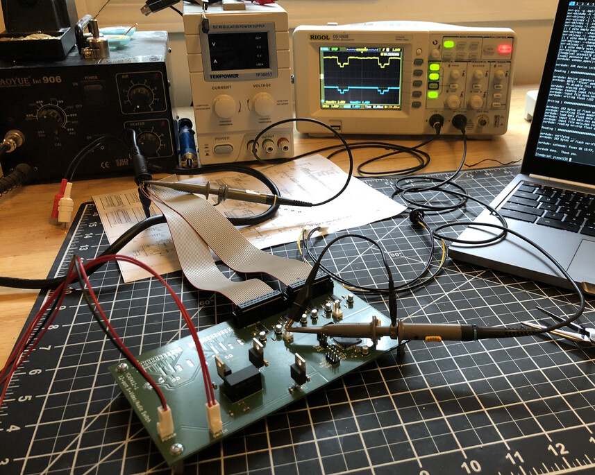
After spending about a month and a half on the planning, designing, and prototyping phases, I had a board, an enclosure, and a big bag of parts. It was time to find out what kind of terrible mistakes I had made in the planning, designing, and prototyping phases.
PCB
When I received the PCBs I was a little surprised at all the empty space - somehow I had imagined it was much more compact. I guess my perception of the relative dimensions in the design in KiCad, even in 3D models, was not accurate. After seeing it in real life, I realized that I could have wasted less space by laying out the digital components in a shorter horizontal strip and compressing the power supply layout to a smaller area. Fortunately, for a one-off project like this, this is mostly an aesthetic concern. I will keep it in mind next time though.
I started soldering components by quadrant, starting with the power supply in the bottom left and moving counter-clockwise, verifying functionality as I went.
I ran into a problem with the video multiplexing. The luminance output matched the source signal, but I couldn’t detect the chroma output on my scope. I realized that while I had intended to terminate each video signal to ground with a 75 Ohm resistor, and had prototyped the design that way, I had completely left the resistors off of the schematic and PCB design. I completely forgot 24 components! Oops!
Well, since the other half of the video input headers are ground, there happened to be a very convenient place to solder the missing resistors on the bottom of the board.
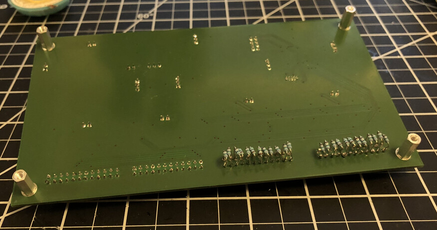
I’m not sure how I would have laid these out if I had remembered to include them in the original design. If there had been a second revision, it would have been fun to try to fit some tiny surface-mount resistors within the header footprint on the bottom of the board.
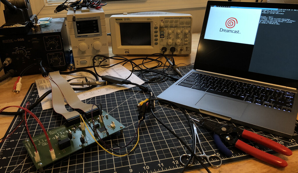
With the terminating resistors in place, the input and output signals looked identical on the scope, so I hooked up the luminance and chroma outputs to a USB video capture device. It looked good!
I also hit a small snag on the audio quadrant. I ordered keyed 24-pin headers, but I had designed for the footprint of bare headers. The keyed headers I ordered did not quite fit, so I had to switch to bare headers for that half of the board. After that, there were no other surprises with the audio, so the board was complete.
Enclosure
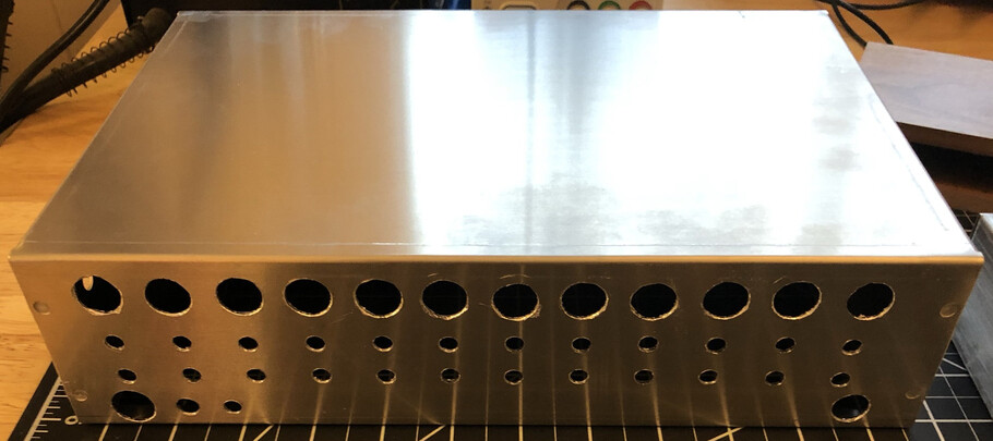
The enclosure needed rectangular cutouts for the power switch and display and tons of holes for mounting screws, the rotary encoder shaft, and the power and A/V connectors on the back.
Front panel
I started by drawing a plan for the front panel on the handy protective covering that came affixed to the enclosure.
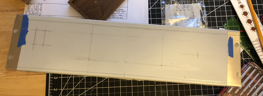
Then I used a nibbler to make the rectangular cutouts. The nibbler was a new tool for me - with a hard squeeze, it removes a 0.1 sq cm of material at a time. It was a lot of work to nibble out the cutouts, but I was surprised by how straight I was able to make them.
I made some mistakes with the front panel. I had trouble making a partial nibble to reach the exact cutout length I needed for the display, and I ended up nibbling a little more than I wanted to. Then to make things worse, I didn’t realize until after I had drilled pilot holes that I had the mounting screw holes rotated 180 degrees, so each mounting screw had a little tiny hole right next to it. It was not turning out well.
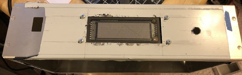
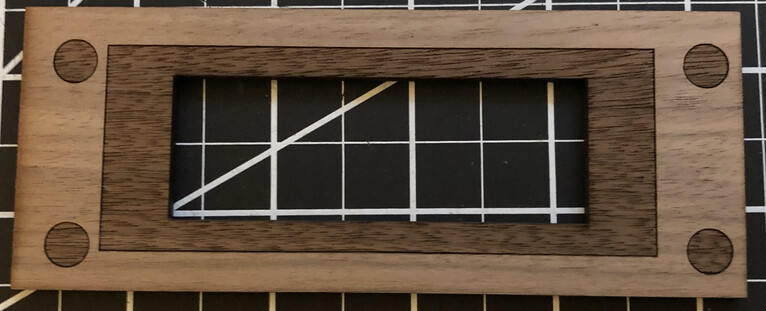
I wasn’t really fond of those mounting screws anyway, so I decided to use a bezel to hide them (and all of my mistakes with the panel cutout). I couldn’t find any existing products that would fit the VFD’s footprint, so I had to make my own. I created a 2D design in LibreCAD and sent it to Ponoko, a laser cutting and engraving service, to have it cut out of a thin piece of walnut to match the enclosure’s paneling.
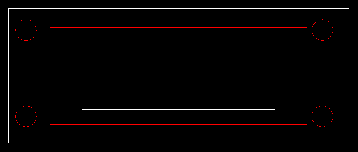
The front of this design is actually the back of the bezel. The white lines in the design are where the material is to be cut, and the red is where it is engraved by burning it with a laser. The screws, even if I used recessed screws, and the display glass stuck out just a little from the plane of the front panel, so I had Ponoko engrave those areas on the back side of the bezel. Their engraving process slightly reduces the thickness of the material in engraved areas, and this would hopefully allow the bezel to fit flush with the enclosure.
While I waited for the bezel to arrive in the mail I got to work on the back panel.
Back panel
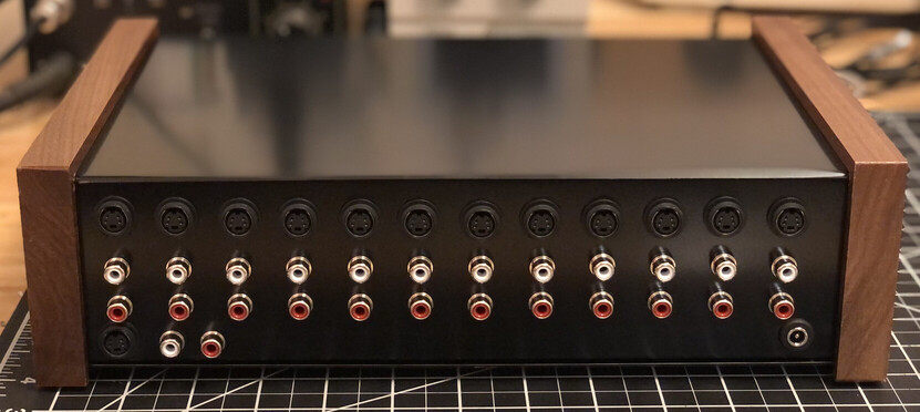
Now that I had some CAD experience, I decided to forego the painstaking pencil and ruler process and to lay out all the connectors in LibreCAD. Then I printed out the design and used it to drill all the pilot holes for 12 sets of A/V connectors and a power jack. You can’t quite see it in the photo below, but there’s a dot in the center of each circle.
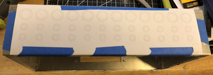
Days after I drilled all of those holes I was doing something completely unrelated when I realized that I actually needed 13 sets of A/V connectors: 12 for the inputs, and 1 for the output. Oops! This was in danger of becoming an 11-port switch, but by sheer luck there was just enough space in the to add a horizontal row of connectors underneath the 12 inputs. This actually isn’t a terrible layout - it makes sense to separate the output connectors from the inputs. You can see the extra holes in the bottom left of this photo.
Finish
I naively thought that I would be able to use the enclosure’s factory aluminum finish, but it turns out that raw aluminum is a poor material for exterior finishes because it oxidizes rapidly and collects fingerprints. I also added a number of surface defects in the process of modifying the enclosure. I’ve never been too happy with the results when I paint things, so I turned to another technique that was entirely new to me: powder-coating. I won’t go into that more, but you can see the results in the next sections. Powder-coating the enclosure was easy, and I really like how it turned out!
Assembly
The next step was a montage of installing the panel-mount components and soldering cables to them.
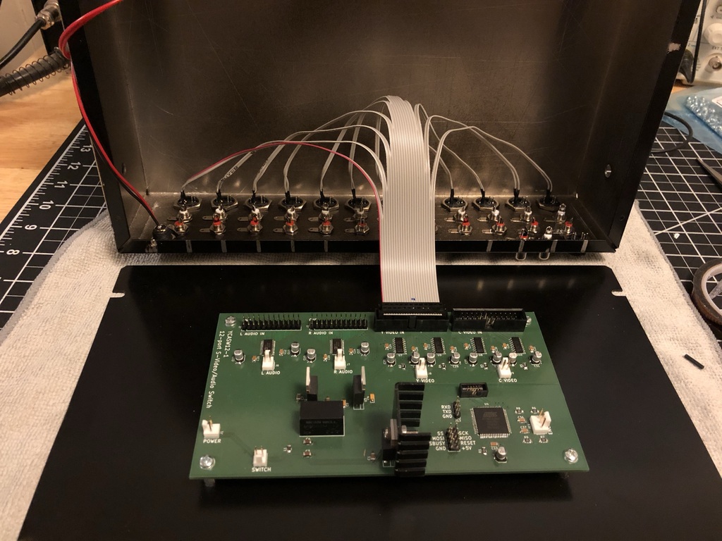
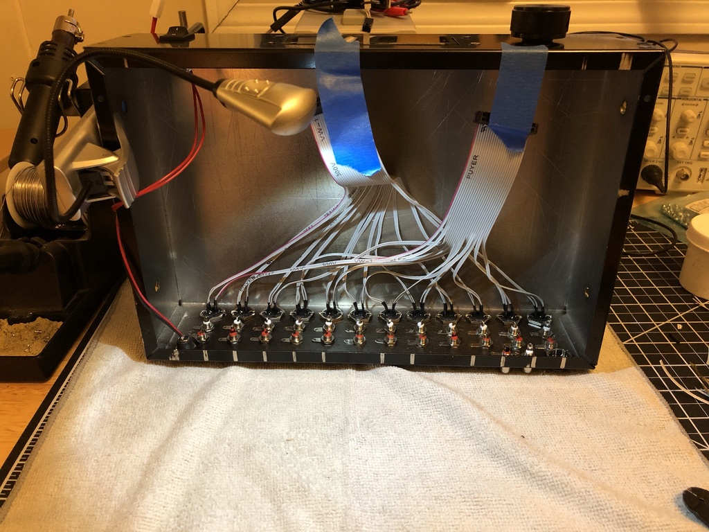
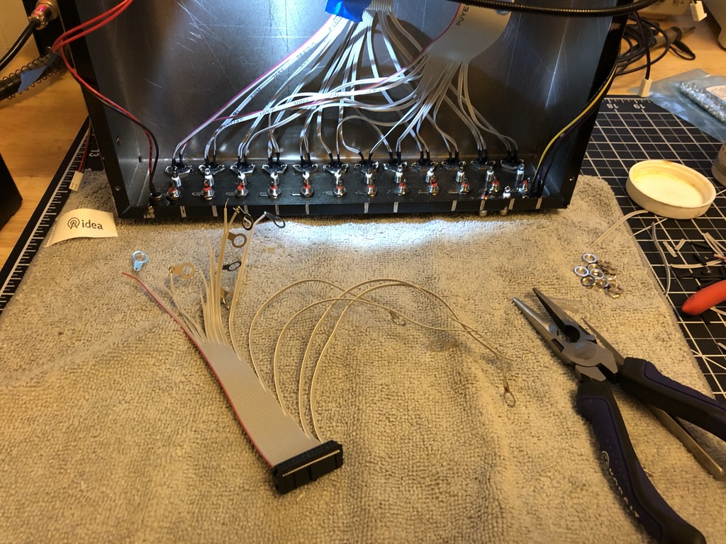
It was tricky cutting each wire of the ribbon cable so it would fan out smoothly from the header on the PCB, and soldering the panel ends and keeping other wires out of the way was tedious. If I had to do this all over again, I might have tried using board-mounted connectors on a PCB mounted to the back panel. I could probably fit all the electronics on the same board or at least an interconnected board stacked against it. Anyway, here’s the completed rat’s nest.
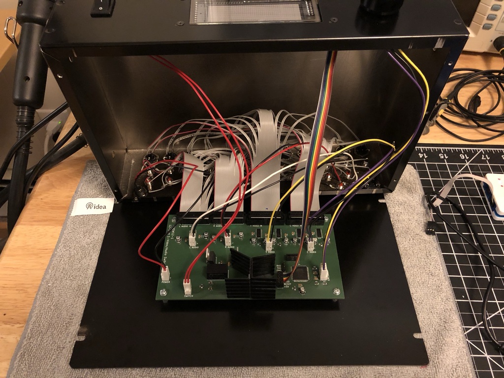
If you look closely through these images, you might notice that one of the voltage regulators gets an increasingly comical mass of heat sinks bolted onto it. Once I started testing more with the VFD, I found that the VFD’s high power consumption makes the +5VD regulator quite hot. Part of this is due to a design flaw. The power dissipation of the regulators depends linearly on the difference between Vin and Vout, so I could have had much less heat if I had used a DC-to-DC converter closer to the minimum Vin of the regulators. I also didn’t plan for the possibility of attaching heat sinks to the regulators, so despite having lots of awkward empty space on the board, there isn’t room to attach them to 2 out of the 3 regulators without bending them out of shape. Something for me to remember next time! Fortunately, with these heat sinks the problem regulator stays cool enough to touch.
With all the electronics assembled, I verified the functionality of each input, and there were no problems.
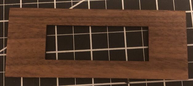
By this time I had received the display bezel in the mail. It fit perfectly around the VFD glass and mounting holes.
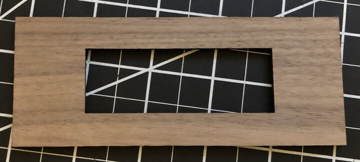
A coat of polyurethane made it match the color of the enclosure’s wood panels pretty closely.
After attaching it to the front panel with some double-sided tape, I had a fully-assembled device.
I have made one “after-market” addition - a ribbon cable that stays plugged in to the JTAG header and hangs out the back of the enclosure so that I can connect a programmer without disconnecting all the cables, opening the enclosure, etc. I will consider building in external programming headers in future projects.
User interface
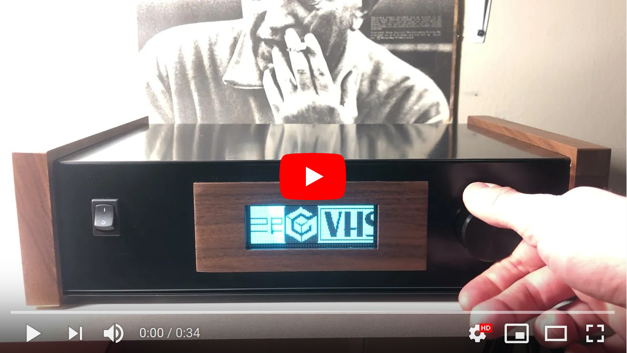
I wanted to create a flashy graphical menu that used product logos to represent each input, but after a few prototypes I identified a couple of especially challenging aspects.
One was the difficulty of fitting recognizable logos onto a monochrome 32-pixel-high display. I decided the menu should be 1-dimensional with only horizontal scrolling in order to maximize the use of vertical space.
The other challenge was the wide variance in logo dimensions. I prototyped different animation and spacing styles that looked fine with logos that had a roughly 1:1 aspect ratio but looked strange when they had to include unusually-wide or -tall logos.
In response to those I designed an interface consisting of a looping horizontal ribbon of variable-width logos. The knob doesn’t change which input is selected - it just moves the position of the sliding window that is the visible portion of the ribbon. Whatever input is nearest the center of the display is the selected input and is highlighted by inverting its colors.

The knob doesn’t directly affect the position either - the window movement has momentum which decays to zero over time, and rotation of the knob just changes the momentum. This gives the interface a very analog feel which you can see in the video linked from the conclusion.
I also added an info menu item which displays total device and per-input uptimes that are persisted to EEPROM, mostly as a way to retroactively justify my decision to use a display and user input instead of using auto-sensing.
Results
I’m now using the switch and have a bunch of things connected to it.
My phone camera doesn’t do the VFD justice, but here’s a short demo of the user interface:
Despite feeling like I had no idea what I was doing most of the time, I think this was overall a success. I was fortunate enough to avoid any mistakes that couldn’t be worked around, and I learned a lot along the way that I can apply to future projects.